Laser Marking Machines in the Electronics Industry
1. Micro-Precision Marking for Miniature Components & PCBs
The relentless miniaturization of consumer electronics—smartphones, wearables, and IoT sensors—demands marking technologies capable of working on surfaces where a single millimeter is wasted space. Lambd fiber and UV laser marking machines deliver micron-level accuracy (up to ±0.001mm), allowing for the engraving of 2D Data Matrix codes, serial numbers, and lot codes on PCB edge traces, capacitor bodies, and connector pins as small as 0201 package size. Unlike inkjet printing which can bridge adjacent contacts or smear, laser marking is a non-contact, dry process that produces crisp, high-contrast characters as small as 0.12mm in height. Lambd's advanced beam shaping and high-resolution galvanometers ensure that even on densely populated multi-layer boards, the mark is placed with pinpoint accuracy without damaging adjacent circuitry, supporting the industry's push toward Industry 4.0 traceability at the component level.
2. "Cold Marking" on Heat-Sensitive Plastics & Silicon with UV Lasers
Electronic components such as IC chips, LCD screens, and flexible printed circuits (FPCs) are highly sensitive to thermal shock. Standard infrared fiber lasers can cause carbonization, melting, or delamination on materials like polycarbonate, ABS, and polyimide film. Lambd UV laser marking systems (355nm wavelength) utilize "cold processing"—a photochemical ablation mechanism that removes material with minimal heat input. This allows for clean, smooth marking on flexible cables, keypad membranes, and semiconductor wafer dicing streets without altering the electrical properties or causing micro-cracks. The result is a permanent, high-contrast mark (often white-on-black or vice versa) that remains legible through reflow soldering and washing processes. For electronics manufacturers, this means zero reject rates due to marking-induced damage, safeguarding both functionality and aesthetics.
3. Permanent Traceability & Compliance (UID, RoHS, CE)
The electronics supply chain is governed by strict regulations including RoHS (Restriction of Hazardous Substances), WEEE, and for defense/medical electronics, MIL-STD-130 UID (Unique Identification). Lambd laser marking machines produce permanent, tamper-evident identifiers that survive reflow ovens, chemical baths, and years of field use. By directly modifying the substrate surface via annealing (metals) or foaming/ablation (plastics), the mark cannot be peeled off like a label. This is critical for tracking counterfeit mitigation, warranty validation, and recall management. Our systems can encode variable data—timestamps, shift codes, and batch IDs—into each mark, which can be linked to an ERP/MES database. This granular traceability ensures that any non-conforming component can be traced back to its exact production origin, fulfilling both legal obligations and customer QA requirements.
4. High-Speed Automation for Mass Production Lines
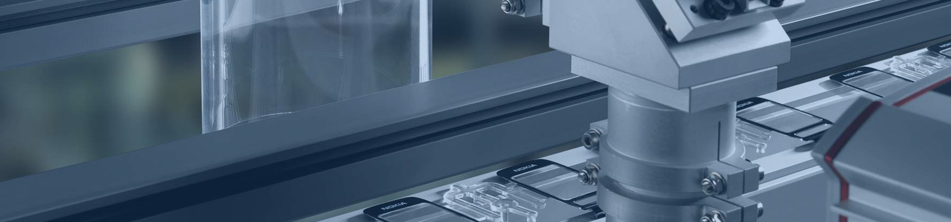
Consumer electronics are produced in volumes exceeding millions of units per month, requiring marking solutions that keep pace without becoming a bottleneck. Lambd laser markers integrate seamlessly with inline conveyors, pick-and-place robots, and vision inspection systems. With marking speeds up to 20,000 mm/s and the ability to fire at frequencies over 100kHz (MOPA models), a single Lambd machine can mark 1,200+ PCBs or casings per minute. The software supports dynamic data import via Ethernet/IP or RS-232, allowing serial numbers to auto-increment in real time. Built-in CCD cameras verify mark presence and readability immediately after lasering, rejecting faulty parts automatically. This closed-loop process eliminates manual verification, reduces labor costs, and ensures 100% data integrity—a necessity for Tier-1 suppliers to Apple, Samsung, and automotive electronics OEMs.
5. Material Versatility: From Bare Metal to Delicate Composites
Electronics manufacturing involves a wide material mix: aluminum heatsinks, brass connectors, stainless steel shielding, gold-plated contacts, silicon wafers, FR4 epoxy boards, and liquid crystal polymer (LCP) housings. Lambd provides multi-wavelength solutions—Fiber (1064nm) for deep engraving on metal shields and annealing on stainless steel; Green (532nm) for marking reflective gold/silver contacts without back-reflection issues; and UV (355nm) for polymers and coated surfaces. MOPA fiber laser options allow users to fine-tune pulse width and frequency to achieve black annealing on stainless steel (no surface relief) or high-contrast color change on anodized parts, all without damaging static-sensitive components. This versatility lets a single marking cell serve multiple product lines, maximizing CAPEX efficiency for EMS (Electronics Manufacturing Services) providers.
Conclusion: Enabling the Connected World, One Mark at a Time
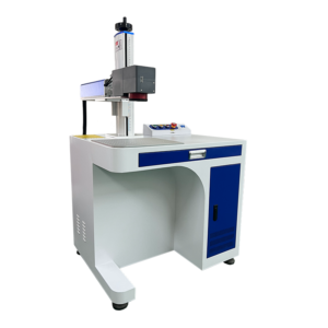
Laser marking in the electronics industry is far more than a cosmetic step—it is the linchpin of component traceability, brand protection, and regulatory compliance. Lambd's specialized fiber and UV laser systems address the unique challenges of this sector: micron-scale precision, zero thermal damage, high-speed automation, and broad material compatibility. By choosing Lambd, electronics manufacturers secure a future-ready marking solution that integrates effortlessly into smart factories, protects product integrity from wafer to finished device, and delivers the permanent, readable codes necessary for global supply chain transparency. In a world where every chip tells a story, we make sure it's written clearly.
Post time: 05-27-2026